
AD5301/AD5311/AD5321 are buffered voltage output 8/10/12-bit DACs from Analog Devices. They support 2.5 V to 5.5 V power supply, operate at 120 mA current, offer I2C®-compatible serial interface, provide data readback capability, have guaranteed monotonicity, low power, power supply derived reference, power-on reset to 0 V, on-chip rail-to-rail output buffer amplifier, and three power-down functions.
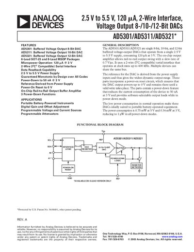
The AD5301, AD5311 and AD5321 are single‑channel buffered voltage‑output DACs available in 8‑, 10‑ and 12‑bit resolutions. They operate from a 2.5 V to 5.5 V supply and feature a 2‑wire serial interface compatible with I²C, supporting clock rates up to 400 kHz. Power‑down mode reduces current consumption to 50 nA at 3 V.
The document provides full electrical characteristics, pin configurations for SOT‑23 and MSOP packages, timing diagrams, ordering information, and mechanical dimensions. It also defines terminology such as relative accuracy, differential nonlinearity, and glitch energy.
| Supply Voltage Range | 2.5 V to 5.5 V |
|---|---|
| Resolution | 8 bits (AD5301), 10 bits (AD5311), 12 bits (AD5321) |
| Power‑Down Current (3 V) | 50 nA |
| Maximum Clock Frequency | 400 kHz |
The devices operate from 2.5 V to 5.5 V.
Power‑down current is 50 nA at 3 V.
AD5301 is 8‑bit, AD5311 is 10‑bit, and AD5321 is 12‑bit.
The serial interface can run up to 400 kHz.