
Key facts
- Brand
- Toshiba
- Model
- TC4001BP
- Industry
- Industrial
- Documents
- 2
- Languages
- EN
- Last added
- 2012-06-07
Start here
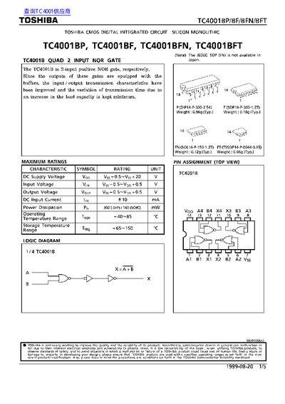
TOSHIBA TC4001BP/BF/BFN/BFT handbook(1)(1)
Datasheet 5 pages · 183 KB · EN
This document is a technical datasheet for the TOSHIBA TC4001B series of CMOS digital integrated circuits. The device functions as a Quad 2-Input Positive NOR Gate and features improved input/output transmission characteristics due to equipped buffers.
The datasheet provides maximum ratings, recommended operating conditions, static and dynamic electrical characteristics, logic diagrams, and outline drawings for four package types: DIP14, SOP14 (200mil), SOP14 (150mil), and TSSOP14.
Toshiba TC4001BP specifications
| Logic Function | Quad 2 Input NOR Gate |
|---|---|
| DC Supply Voltage (Vop) | -0.5 to Vs5 + 20 V |
| Operating Temperature Range (opr) | -40 to 85 °C |
| Storage Temperature Range (Tstg) | -65 to 150 C |
| Propagation Delay Time (tPHL) at Vcc=5V | Max. 200 ns |
| Input Capacitance (Cin) | Max. 75 pF |
All Toshiba TC4001BP documents by type
Datasheet 2
Ratings, dimensions and ordering codes, for selection and design work.
Questions answered in these manuals
What is the maximum DC supply voltage for the TC4001B?
The maximum DC supply voltage rating is +5.5 V.
What is the typical weight of a TC4001B in a DIP package?
A DIP package typically weighs 0.96g.
What is the maximum DC supply voltage for this gate?
The maximum DC supply voltage rating is 18 V.
How much does a typical DIP package weigh?
A typical DIP package weighs 0.96g.