
Key facts
- Brand
- Analog Devices
- Model
- AD9513
- Industry
- Industrial
- Documents
- 2
- Languages
- EN
- Last added
- 2012-05-03
Start here
Analog Devices AD9513 Clock Distribution IC Datasheet
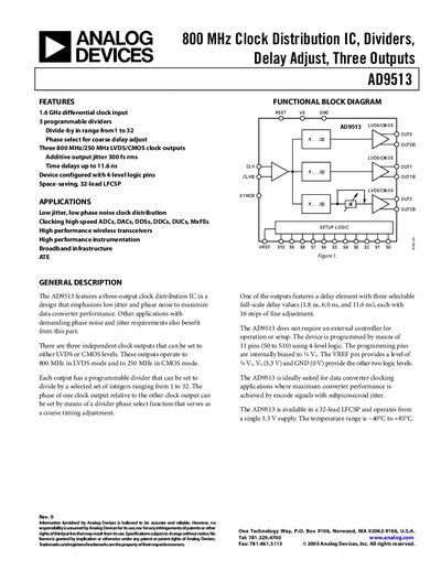
The AD9513 provides three independent clock outputs that can be configured as LVDS (up to 800 MHz) or CMOS (up to 250 MHz). Each output includes a programmable divider (1‑to‑32) and a coarse phase‑select delay, with a selectable fine‑adjustable delay up to 11.6 ns. The device operates from a single 3.3 V supply and is packaged in a 32‑lead LFCSP.
Typical applications include high‑speed ADC/DAC clocking, wireless transceivers, instrumentation, and broadband test equipment. The datasheet details functional block diagrams, pin configurations, timing characteristics, phase‑noise and jitter performance, power‑management options, and layout recommendations for optimal low‑jitter operation.
Analog Devices AD9513 specifications
| Clock Input Frequency Range | 0 – 1.6 GHz |
|---|---|
| LVDS Clock Output Frequency | 0 – 800 MHz |
| CMOS Clock Output Frequency | 0 – 250 MHz |
| Additive Output Jitter | 300 fs rms |
| Supply Voltage | 3.3 V ± 5% |
| Operating Temperature Range | -40 °C to +85 °C |
| Package | 32‑lead LFCSP |
Source: Analog Devices AD9513 Clock Distribution IC Datasheet
All Analog Devices AD9513 documents by type
Ratings, dimensions and ordering codes, for selection and design work.
Questions answered in these manuals
What is the maximum LVDS output frequency of the AD9513?
The LVDS outputs can operate up to 800 MHz.
What supply voltage does the AD9513 require?
It requires a 3.3 V ± 5% supply.
What is the maximum clock input frequency of the AD9513?
The AD9513 accepts a clock input up to 1.6 GHz.
How many programmable dividers does the AD9513 provide and what range can they be set to?
It provides three programmable dividers with a divide‑by range from 1 to 32.