
This datasheet provides SN54LVC541A and SN74LVC541A octal buffer/driver features, including pinout, package, input voltage, output voltage, operating voltage range, pull current, package etc.
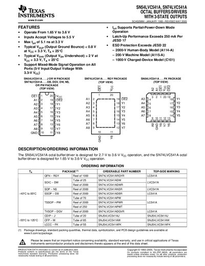
The SN54LVC541A and SN74LVC541A are octal buffer/driver devices designed for low‑voltage operation with 3‑state outputs. The SN54LVC541A operates from 2.7 V to 3.6 V VCC, while the SN74LVC541A supports a wider range of 1.65 V to 3.6 V VCC. Both devices feature partial‑power‑down mode, mixed‑mode signal operation, and ESD protection exceeding industry standards.
The document provides detailed ordering information, absolute maximum ratings, recommended operating conditions, electrical and switching characteristics, as well as packaging and mechanical data. It also includes an important notice on product availability and warranty.
| Supply voltage (SN54LVC541A) | 2.7 V to 3.6 V VCC |
|---|---|
| Supply voltage (SN74LVC541A) | 1.65 V to 3.6 V VCC |
| Typical propagation delay | 5.1 ns at 3.3 V |
| Output current capability | Up to 250 mA per pin |
| ESD protection | 2000 V Human‑Body Model, 200 V Machine Model, 1000 V Charged‑Device Model |
It is a 2‑input AND gate with active‑low inputs; if either output‑enable input is high, all eight outputs go to high‑impedance.
Tie OE to VCC through a pull‑up resistor; the resistor value must be chosen based on the driver’s current‑sinking capability.
For the SN54LVC541A: –55 °C to 125 °C; for the SN74LVC541A: –40 °C to 85 °C.