
Key facts
- Brand
- Motorola
- Model
- MC100E167
- Industry
- Industrial
- Documents
- 2
- Languages
- EN
- Last added
- 2012-07-09
Start here
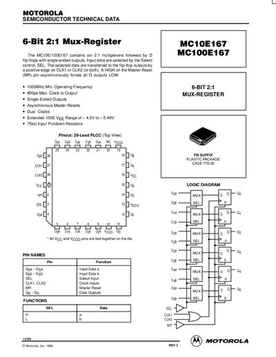
Motorola MC10E167/MC100E167 6-Bit 2:1 Mux-Register Datasheet
This document is a technical datasheet for the Motorola MC10E167 and MC100E167 integrated circuits. The device contains six 2:1 multiplexers followed by D flip-flops with single-ended outputs. Data selection is controlled by the SEL pin, and data is transferred to the outputs on a positive edge of the CLK1 or CLK2 clock inputs. An asynchronous Master Reset (MR) pin forces all outputs LOW.
Read onlineMotorola MC100E167 specifications
| Operating Frequency | 1000MHz Min. |
|---|---|
| Clock to Output Delay | 800ps Max. |
| Package Type | 28-Lead PLCC |
| Supply Voltage Range (100E) | -4.2V to -5.46V |
| Input Pulldown Resistors | 75kQ |
| Max. Toggle Frequency | 1000 MHz |
Source: Motorola MC10E167/MC100E167 6-Bit 2:1 Mux-Register Datasheet
All Motorola MC100E167 documents by type
Ratings, dimensions and ordering codes, for selection and design work.
Questions answered in these manuals
How are the outputs transferred?
The selected data are transferred to the flip-flop outputs by a positive edge on CLK1 or CLK2.
From: Motorola MC10E167/MC100E167 6-Bit 2:1 Mux-Register Datasheet
What does the Master Reset pin do?
A HIGH on the Master Reset (MR) pin asynchronously forces all Q outputs LOW.
From: Motorola MC10E167/MC100E167 6-Bit 2:1 Mux-Register Datasheet
What is the function of the MR pin?
A HIGH on the Master Reset (MR) pin asynchronously forces all Q outputs LOW.
How is data transferred to the flip-flop outputs?
The selected data are transferred by a positive edge on CLK1 or CLK2.