
The MC10E/100E167 contains six 2:1 multiplexers followed by D flip-flops with single-ended outputs. Input data are selected by the Select control, SEL. The selected data are transferred to the flip-flop outputs by a positive edge on CLK1 or CLK2 (or both). A HIGH on the Master Reset (MR) pin asynchronously forces all Q outputs LOW.
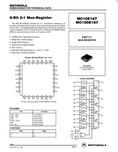
This document is a technical datasheet for the Motorola MC10E167 and MC100E167 integrated circuits. The device contains six 2:1 multiplexers followed by D flip-flops with single-ended outputs. Data selection is controlled by the SEL pin, and data is transferred to the outputs on a positive edge of the CLK1 or CLK2 clock inputs. An asynchronous Master Reset (MR) pin forces all outputs LOW.
| Operating Frequency | 1000MHz Min. |
|---|---|
| Clock to Output Delay | 800ps Max. |
| Package Type | 28-Lead PLCC |
| Supply Voltage Range (100E) | -4.2V to -5.46V |
| Input Pulldown Resistors | 75kQ |
| Max. Toggle Frequency | 1000 MHz |
The selected data are transferred to the flip-flop outputs by a positive edge on CLK1 or CLK2.
A HIGH on the Master Reset (MR) pin asynchronously forces all Q outputs LOW.
The minimum operating frequency is 1000MHz.