
Key facts
- Brand
- Toshiba
- Model
- 2SK2613
- Industry
- Industrial
- Documents
- 4
- Languages
- EN
- Last added
- 2012-04-01
Start here
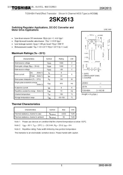
TOSHIBA 2SK2613 Manual(3)
The Toshiba 28K2613 is an N‑channel silicon field‑effect transistor designed for switching regulator, DC‑DC converter, and motor‑drive applications. It features a low drain‑source on‑resistance and high forward transfer admittance.
The document lists detailed electrical parameters, thermal characteristics, and recommended handling procedures. It also defines the intended usage scope and restrictions for safety‑critical applications.
Toshiba 2SK2613 specifications
| Drain‑source voltage (VDS) | 1000 V |
|---|---|
| On‑resistance (RDS(on)) | 1.4 (typ.) |
| Gate threshold voltage (Vth) | 2.0 – 4.0 V |
| Continuous drain current (Id) | 8 A |
| Storage temperature range | -55 °C to 150 °C |
Source: TOSHIBA 2SK2613 Manual(2)
All Toshiba 2SK2613 documents by type
Ratings, dimensions and ordering codes, for selection and design work.
Questions answered in these manuals
What is the maximum drain‑source voltage for the Toshiba 28K2613?
The device can withstand up to 1000 V drain‑source voltage.
What is the typical on‑resistance of the 28K2613 MOSFET?
The typical on‑resistance is 1.4 (typ.).
What is the maximum drain‑source voltage for the 2SK2613?
The device can withstand up to 1000 V between drain and source.
What is the typical on‑resistance of the 2SK2613?
Typical RDS(ON) is 1.4 Ω at VGS = 10 V and ID = 4 A.
What is the maximum drain‑source voltage for the 2SK2613?
The device can withstand up to 1000 V between drain and source.
How should the 2SK2613 be handled to avoid damage?
It is an electrostatic‑sensitive device and should be handled with caution.