
Key facts
- Brand
- Toshiba
- Model
- 2SK2611
- Industry
- Industrial
- Documents
- 3
- Languages
- EN
- Last added
- 2012-04-01
Start here
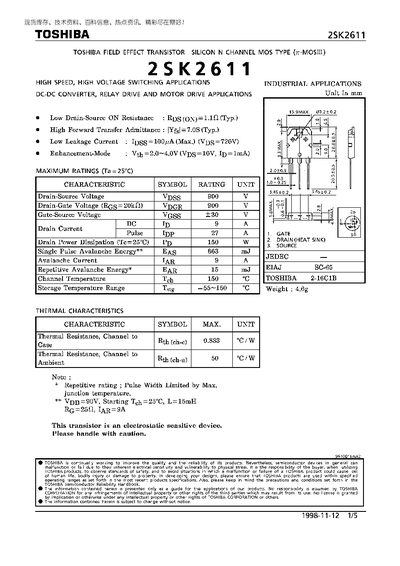
Toshiba 2SK2611 N-Channel MOSFET Datasheet
The Toshiba 2SK2611 is a silicon N‑channel MOSFET designed for high‑speed, high‑voltage switching applications such as DC‑DC converters, relay drives and motor drives. It is an enhancement‑mode device with a typical on‑resistance of 1.10 mΩ and can handle up to 9 A continuous drain current.
Key electrical specifications include a maximum drain‑source voltage of 900 V, a gate‑source voltage rating of +30 V, and a maximum power dissipation of 150 W at 25 °C. Thermal resistance from channel to case is 0.833 °C/W, and the device is rated for storage temperatures from –55 °C to 150 °C.
Toshiba 2SK2611 specifications
| Drain‑Source Voltage (VDS) | 900 V (max) |
|---|---|
| Gate‑Source Voltage (VGS) | +30 V (max) |
| Continuous Drain Current (ID) | 9 A (max) |
| On‑Resistance (RDS(on)) | 1.10 mΩ (typ) |
| Power Dissipation (PD) | 150 W (max) |
| Storage Temperature Range | -55 °C to 150 °C |
All Toshiba 2SK2611 documents by type
Ratings, dimensions and ordering codes, for selection and design work.
Questions answered in these manuals
What is the maximum drain‑source voltage of the Toshiba 2SK2611?
The device can withstand up to 900 V between drain and source.
What is the typical on‑resistance of the 2SK2611?
Its typical on‑resistance is 1.10 mΩ.
What is the maximum drain‑source voltage for the Toshiba 2SK2611?
The device can withstand up to 900 V between drain and source.
What is the typical on‑resistance of the 2SK2611?
The typical on‑resistance is 1.1 Ω.
What is the maximum drain‑source voltage for the Toshiba 2SK2611?
The device is rated for a maximum drain‑source voltage of 900 V.
What is the typical on‑resistance of the 2SK2611 MOSFET?
Its typical on‑resistance is 1.1 Ω (max 1.4 Ω).