
The 2SK2613 is a N-channel MOS type field effect transistor manufactured by TOSHIBA, suitable for switching power supplies, DC-DC converters and motor drive applications.
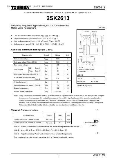
The Toshiba 2SK2613 is an N‑channel MOSFET designed for switching regulator, DC‑DC converter and motor‑drive applications. The document provides absolute maximum ratings, typical electrical parameters, and thermal characteristics for reliable design use.
Key sections cover absolute maximum ratings, detailed electrical characteristics such as drain‑source voltage, on‑resistance and gate charge, thermal resistance values, and product‑use restrictions with handling precautions for this electrostatic‑sensitive device.
| Drain‑source voltage (VDSS) | 1000 V |
|---|---|
| Gate‑source voltage (VGSS) | ±30 V |
| On‑resistance (RDS(ON), typical) | 1.4 Ω |
| Forward transfer admittance (|Yfs|, typical) | 6.0 S |
| Leakage current (IDSS, max) | 100 µA |
| Gate threshold voltage (Vth, typical) | 2.0‑4.0 V |
| Thermal resistance, channel‑to‑case (Rth(ch‑c)) | 0.833 °C/W |
| Thermal resistance, channel‑to‑ambient (Rth(ch‑a)) | 50 °C/W |
The device can withstand up to 1000 V between drain and source.
Typical RDS(ON) is 1.4 Ω at VGS = 10 V and ID = 4 A.
It must be handled with caution, using proper ESD protection and following the handling guide in the Toshiba Semiconductor Reliability Handbook.
Rth(ch‑c) is 0.833 °C/W and Rth(ch‑a) is 50 °C/W.