
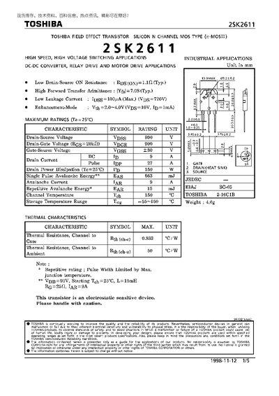
The Toshiba 2SK2611 is a silicon N‑channel MOSFET designed for high‑speed, high‑voltage switching applications such as DC‑DC converters, relay drives and motor drives. It is an enhancement‑mode device with a typical on‑resistance of 1.10 mΩ and can handle up to 9 A continuous drain current.
Key electrical specifications include a maximum drain‑source voltage of 900 V, a gate‑source voltage rating of +30 V, and a maximum power dissipation of 150 W at 25 °C. Thermal resistance from channel to case is 0.833 °C/W, and the device is rated for storage temperatures from –55 °C to 150 °C.
| Drain‑Source Voltage (VDS) | 900 V (max) |
|---|---|
| Gate‑Source Voltage (VGS) | +30 V (max) |
| Continuous Drain Current (ID) | 9 A (max) |
| On‑Resistance (RDS(on)) | 1.10 mΩ (typ) |
| Power Dissipation (PD) | 150 W (max) |
| Storage Temperature Range | -55 °C to 150 °C |
The device can withstand up to 900 V between drain and source.
Its typical on‑resistance is 1.10 mΩ.
The transistor is rated for a continuous drain current of 9 A.
It can be stored from –55 °C up to 150 °C.