
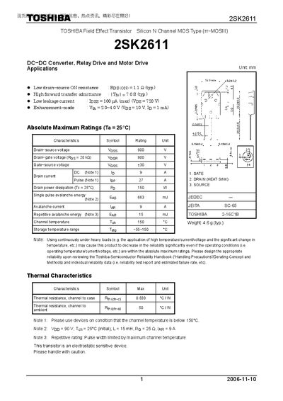
The Toshiba 2SK2611 is a silicon N‑channel MOSFET designed for DC‑DC converters, relay drive and motor drive applications. The document provides absolute maximum ratings, electrical characteristics, thermal data, and handling precautions.
Key sections include Absolute Maximum Ratings, Electrical Characteristics, Thermal Characteristics, Marking information, and product‑use restrictions. The device is lead‑free and intended for general electronics use, with specific warnings for high‑reliability or safety‑critical applications.
| Drain‑source voltage (VDS) | 900 V |
|---|---|
| Gate‑source voltage (VGS) max | 30 V |
| On‑resistance (RDS(on)) typical | 1.1 Ω |
| Input capacitance (Ciss) | 2040 pF |
| Output capacitance (Coss) | 190 pF |
| Weight | 4.6 g (typ.) |
| Storage temperature range | -55 °C to 150 °C |
| Thermal resistance, channel‑to‑case (Rth(ch‑c)) | 0.833 °C·W |
The device can withstand up to 900 V between drain and source.
The typical on‑resistance is 1.1 Ω.
It can be stored from –55 °C up to 150 °C.
Yes, the marking indicates a lead‑free package or finish.