
Key facts
- Brand
- Fairchild
- Model
- FQPF2P40
- Industry
- Industrial
- Documents
- 2
- Languages
- EN
- Last added
- 2012-04-12
Start here
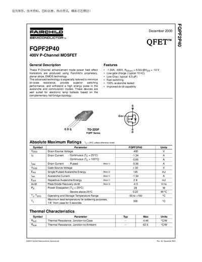
Fairchild FQPF2P40 400V P-Channel MOSFET Datasheet
The FQPF2P40 is a P‑Channel enhancement‑mode power MOSFET fabricated with Fairchild’s planar stripe DMOS technology. It is optimized for low on‑state resistance, fast switching, and high‑energy avalanche performance, making it suitable for electronic lamp ballast applications using complementary half‑bridge topologies.
Key electrical characteristics include a -400 V drain‑source rating, -1.34 A continuous drain current at 25 °C, low gate charge (~10 nC), low reverse transfer capacitance (≈6.5 pF), and a maximum power dissipation of 28 W. The device is supplied in a TO‑220F package with thermal resistance values of 4.46 °C·W (junction‑to‑case) and 62.5 °C·W (junction‑to‑ambient).
Fairchild FQPF2P40 specifications
| Drain‑Source Voltage (VDS) | -400 V |
|---|---|
| Continuous Drain Current (ID) at 25 °C | -1.34 A |
| Gate‑Source Voltage (VGS) | +30 V |
| Total Gate Charge (Qg) | 10 nC (typical) |
| Reverse Transfer Capacitance (Crss) | 6.5 pF (typical) |
| Maximum Power Dissipation (P_D) at 25 °C | 28 W |
| Thermal Resistance, Junction‑to‑Case (RθJC) | 4.46 °C·W |
| Avalanche Energy (EAS) | 120 mJ |
All Fairchild FQPF2P40 documents by type
Ratings, dimensions and ordering codes, for selection and design work.
Questions answered in these manuals
What is the maximum drain‑source voltage rating of the FQPF2P40?
The device is rated for a maximum drain‑source voltage of -400 V.
What is the typical gate charge for this MOSFET?
The typical total gate charge is about 10 nC.
What is the maximum drain‑source voltage for the FQPF2P40?
The device can withstand a drain‑source voltage of up to –400 V.
What is the typical gate charge of the FQPF2P40?
The typical total gate charge is 10 nC.