
Key facts
- Brand
- Analog Devices
- Model
- ADN4668
- Industry
- Industrial
- Documents
- 2
- Languages
- EN
- Last added
- 2012-05-07
Start here
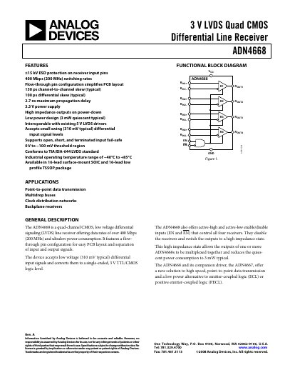
Analog Devices ADN4668 Quad LVDS CMOS Differential Line Receiver Datasheet
The ADN4668 is a four‑channel LVDS line receiver that converts low‑voltage differential inputs (typical 310 mV) to 3 V TTL/CMOS logic levels. It features a flow‑through pin configuration for easy PCB layout, active‑high and active‑low enable inputs, and ultra‑low quiescent current (≈3 mW typical).\n\nDesigned for point‑to‑point data transmission, multidrop buses, clock distribution and backplane applications, the device is available in 16‑lead SOIC and TSSOP packages and operates over an industrial temperature range (‑40 °C to +85 °C).
Read onlineAnalog Devices ADN4668 specifications
| Maximum data rate | 400 Mbps (200 MHz) |
|---|---|
| Supply voltage range | 3.0 V to 3.6 V |
| Maximum propagation delay | 2.7 ns |
| Output high voltage | 2.7 V to 3.3 V |
| ESD protection | ±15 kV on receiver input pins |
Source: Analog Devices ADN4668 Quad LVDS CMOS Differential Line Receiver Datasheet
All Analog Devices ADN4668 documents by type
Ratings, dimensions and ordering codes, for selection and design work.
Questions answered in these manuals
What is the maximum data rate of the ADN4668?
The device supports data rates of over 400 Mbps (200 MHz) switching rates.
From: Analog Devices ADN4668 Quad LVDS CMOS Differential Line Receiver Datasheet
What supply voltage range does the ADN4668 operate over?
It operates from 3.0 V to 3.6 V supply voltage.
From: Analog Devices ADN4668 Quad LVDS CMOS Differential Line Receiver Datasheet
What is the maximum data rate of the ADN4668?
The device supports data rates up to 400 Mbps (200 MHz).
What supply voltage does the ADN4668 require?
It operates from a 3.3 V power supply.