
The 3 V LVDS Quad CMOS Differential Line Receiver ADN4668 is a four-channel CMOS differential line receiver from Analog Devices. It has a 3.3 V power supply, supports 400 Mbps (200 MHz) switching rates, and has ±15 kV ESD protection on the receiver input pins. It supports small swing (310 mV typical) differential input signal levels, supports open, short, and terminated input fail-safe, and conforms to the TIA/EIA-644 LVDS standard.
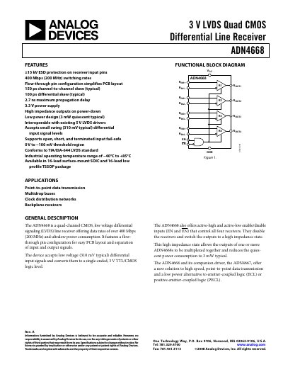
The ADN4668 is a four‑channel LVDS line receiver that converts low‑voltage differential inputs (typical 310 mV) to 3 V TTL/CMOS logic levels. It features a flow‑through pin configuration for easy PCB layout, active‑high and active‑low enable inputs, and ultra‑low quiescent current (≈3 mW typical).\n\nDesigned for point‑to‑point data transmission, multidrop buses, clock distribution and backplane applications, the device is available in 16‑lead SOIC and TSSOP packages and operates over an industrial temperature range (‑40 °C to +85 °C).
| Maximum data rate | 400 Mbps (200 MHz) |
|---|---|
| Supply voltage range | 3.0 V to 3.6 V |
| Maximum propagation delay | 2.7 ns |
| Output high voltage | 2.7 V to 3.3 V |
| ESD protection | ±15 kV on receiver input pins |
The device supports data rates of over 400 Mbps (200 MHz) switching rates.
It operates from 3.0 V to 3.6 V supply voltage.
The receiver input pins are protected against ±15 kV ESD events.
The ADN4668 has both active‑high and active‑low enable inputs that place the outputs in a high‑impedance state when disabled.