
Key facts
- Brand
- Analog Devices
- Model
- ADN2806
- Industry
- Electronics
- Documents
- 2
- Languages
- EN
- Last added
- 2012-05-03
Start here
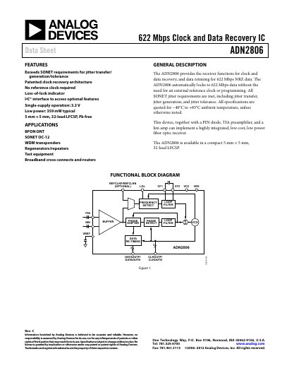
Analog Devices ADN2806 Clock and Data Recovery IC Data Sheet
The ADN2806 is a 622 Mbps clock and data recovery IC that automatically locks to incoming data without an external reference clock. It meets SONET jitter requirements and offers low‑power single‑supply operation in a compact 5 mm × 5 mm, 32‑lead LFCSP package.
The document provides feature highlights, application examples, full electrical specifications, pin descriptions, I²C register map, PCB design guidelines, and ordering information for designers integrating the device into fiber‑optic receivers and high‑speed communication systems.
Analog Devices ADN2806 specifications
| Input Voltage Range (PIN/NIN) | 1.8 V – 2.8 V |
|---|---|
| Power Supply Voltage (VCC) | 3.0 V – 3.6 V |
| Operating Temperature Range | –40 °C to +85 °C |
| Output Voltage High (VOH) | 1.475 V |
| Loss‑of‑Lock (LOL) Response Time | 200 µs |
| I²C Clock Frequency | Up to 400 kHz |
| Package Size | 5 mm × 5 mm, 32‑lead LFCSP |
Source: Analog Devices ADN2806 Clock and Data Recovery IC Data Sheet
All Analog Devices ADN2806 documents by type
Ratings, dimensions and ordering codes, for selection and design work.
Questions answered in these manuals
What is the input voltage range for the ADN2806?
The device accepts a differential input voltage between 1.8 V and 2.8 V.
From: Analog Devices ADN2806 Clock and Data Recovery IC Data Sheet
Does the ADN2806 require an external reference clock?
No, the chip automatically locks to the incoming 622 Mbps data without an external reference clock.
From: Analog Devices ADN2806 Clock and Data Recovery IC Data Sheet
Does the ADN2806 require an external reference clock?
No, the device locks to the data stream without a reference clock.
What is the maximum data rate supported by the ADN2806?
The device operates at 622 Mbps.