
The ADN2806 is a receiver that provides clock and data recovery for 622 Mbps NRZ data. It exceeds SONET requirements for jitter transfer/generation/tolerance, does not require an external reference clock, has a loss-of-lock indicator, and has an I2C interface for accessing optional features. It operates on a single supply voltage and has low power consumption.
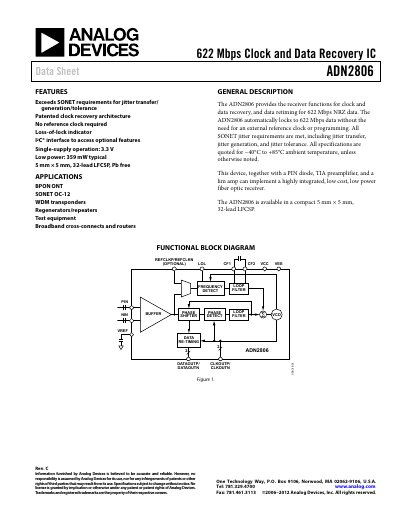
The ADN2806 is a 622 Mbps clock and data recovery IC that automatically locks to incoming data without an external reference clock. It meets SONET jitter requirements and offers low‑power single‑supply operation in a compact 5 mm × 5 mm, 32‑lead LFCSP package.
The document provides feature highlights, application examples, full electrical specifications, pin descriptions, I²C register map, PCB design guidelines, and ordering information for designers integrating the device into fiber‑optic receivers and high‑speed communication systems.
| Input Voltage Range (PIN/NIN) | 1.8 V – 2.8 V |
|---|---|
| Power Supply Voltage (VCC) | 3.0 V – 3.6 V |
| Operating Temperature Range | –40 °C to +85 °C |
| Output Voltage High (VOH) | 1.475 V |
| Loss‑of‑Lock (LOL) Response Time | 200 µs |
| I²C Clock Frequency | Up to 400 kHz |
| Package Size | 5 mm × 5 mm, 32‑lead LFCSP |
The device accepts a differential input voltage between 1.8 V and 2.8 V.
No, the chip automatically locks to the incoming 622 Mbps data without an external reference clock.
The I²C interface operates up to 400 kHz.
It is supplied in a 5 mm × 5 mm, 32‑lead LFCSP package.