
The ADN2806 is a clock and data recovery IC produced by Analog Devices. It meets SONET jitter transfer/generation/tolerance requirements, and does not require a reference clock. It has a patented clock recovery architecture, low power consumption and other features, making it very suitable for applications such as BPON ONT, SONET OC-12 WDM transponders, Regenerators/repeaters, Test equipment and Broadband cross-connects and routers.
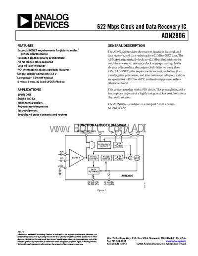
The ADN2806 is a 622 Mbps clock and data recovery IC that automatically locks to incoming NRZ data without an external reference clock. It meets SONET jitter requirements for transfer, generation, and tolerance, and includes a loss‑of‑lock indicator and optional PC interface.
The document provides full electrical specifications, pin descriptions, timing diagrams, and ordering information for the 5 mm × 5 mm 32‑lead LFCSP package, along with jitter performance data and thermal characteristics.
| Data Rate | 622 Mbps |
|---|---|
| Power Supply Voltage | 3.0 V – 3.6 V |
| Power Supply Current (locked) | 109 mA |
| Operating Temperature Range | -40 °C to +85 °C |
| Input Voltage Range (PIN/NIN) | 1.8 V – 2.8 V |
| Input Resistance Differential | 100 Ω |
| LVDS Output Voltage High | 1.475 V |
| Differential Output Swing | 250 mV – 400 mV |
| Jitter Transfer Bandwidth (OC‑12) | 75 kHz – 130 kHz |
| Package | 5 mm × 5 mm, 32‑lead LFCSP |
No, the device locks to the data stream without a reference clock.
The device operates at 622 Mbps.
It operates from –40 °C to +85 °C.
It is supplied in a 5 mm × 5 mm, 32‑lead LFCSP.