
Key facts
- Brand
- Analog Devices
- Model
- ADN2805
- Industry
- Industrial
- Documents
- 2
- Languages
- EN
- Last added
- 2012-05-03
Start here
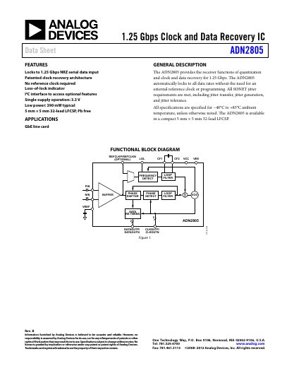
Analog Devices ADN2805 Data Sheet Rev B
The ADN2805 is a 1.25 Gbps clock and data recovery integrated circuit that provides receiver functions such as quantization, clock recovery, and loss‑of‑lock indication without requiring an external reference clock. It is targeted for GbE line‑card applications and operates over a temperature range of –40 °C to +85 °C.
The document includes features, applications, detailed electrical specifications, pin configuration, I²C register interface, SQUELCH mode operation, PCB design guidelines, and thermal and absolute‑maximum ratings. Key sections such as the functional block diagram, jitter specifications, and output timing are presented with tables and figures.
Analog Devices ADN2805 specifications
| Data Rate | 1250 Mbps |
|---|---|
| Power Supply Voltage | 3.0 – 3.6 V |
| Power Supply Current | 118 – 131 mA |
| Operating Temperature Range | -40 °C to +85 °C |
| LVDS Output Swing (VOD) | 240 – 400 mV |
| Output Impedance | 100 Ω |
| I2C Clock Frequency | 400 kHz |
| Package Size | 5 mm × 5 mm |
All Analog Devices ADN2805 documents by type
Ratings, dimensions and ordering codes, for selection and design work.
Questions answered in these manuals
What is the maximum data rate supported by the ADN2805?
The ADN2805 supports a data rate of up to 1.25 Gbps (1250 Mbps).
Does the ADN2805 require an external reference clock?
No, the device locks to the incoming data stream without an external reference clock.
Does the ADN2805 require an external reference clock?
No, the ADN2805 automatically locks to all data rates without the need for an external reference clock.
From: Analog Devices ADN2805 Clock and Data Recovery IC Datasheet
What is the maximum data rate supported by the ADN2805?
The device supports a data rate of 1.25 Gbps (1250 Mbps).
From: Analog Devices ADN2805 Clock and Data Recovery IC Datasheet