
Key facts
- Brand
- Analog Devices
- Model
- ADUC7121
- Industry
- Industrial
- Documents
- 2
- Languages
- EN
- Last added
- 2012-05-03
Start here
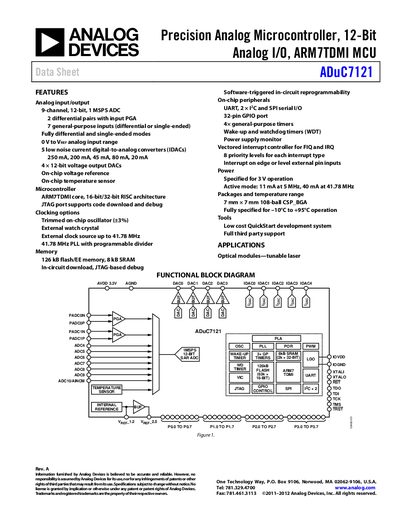
Analog Devices ADuC7121 Product Handbook Rev A
The ADuC7121 is a fully integrated 12‑bit microcontroller featuring a 9‑channel, 1 MSPS ADC, five current‑output DACs, four voltage‑output DACs, and an ARM7TDMI core with up to 41 MIPS performance. It operates from 3.0 V to 3.6 V and is specified for industrial temperatures from –10 °C to +95 °C.
The handbook provides detailed specifications, functional block diagrams, pin configurations, timing data, and information on the on‑chip peripherals such as UART, SPI, PWM, timers, and power‑supply monitoring. It also includes revision history, ordering guide, and package dimensions for the 108‑ball CSP‑BGA package.
Analog Devices ADUC7121 specifications
| ADC resolution | 12 bits |
|---|---|
| ADC sampling rate | 1 MSPS |
| Flash memory | 126 kB |
| SRAM | 8 kB |
| Operating voltage | 3.0 V to 3.6 V |
| Temperature range | -10 °C to +95 °C |
| IDAC0 full‑scale output | 250 mA |
| IDAC1 full‑scale output | 200 mA |
| IDAC2 full‑scale output | 45 mA |
| IDAC3 full‑scale output | 80 mA |
| IDAC4 full‑scale output | 20 mA |
| PLL frequency | 41.78 MHz |
All Analog Devices ADUC7121 documents by type
Ratings, dimensions and ordering codes, for selection and design work.
How to use the product for one specific task, with worked examples.
Questions answered in these manuals
What is the ADC resolution of the ADuC7121?
The ADC provides a 12‑bit resolution.
What is the operating voltage range for the ADuC7121?
It operates from 3.0 V to 3.6 V.
What must be ensured for SPI clock pulses when the ADuC7121 is in slave mode?
The number of clock pulses from the master must be divisible by 8 while the chip‑select pin is low.
What occurs if the I²C slave interface is disabled while a transfer is in progress?
The ADuC7121 may drive the SDA pins low indefinitely until a hardware reset occurs.