
Key facts
- Brand
- Analog Devices
- Model
- ADCLK914
- Industry
- Industrial
- Documents
- 2
- Languages
- EN
- Last added
- 2012-05-03
Start here
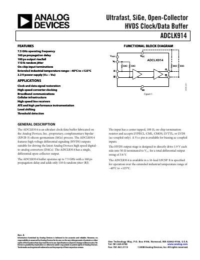
Analog Devices ADCLK914 Clock/Data Buffer Datasheet
The ADCLK914 is a high‑speed clock and data buffer fabricated on Analog Devices' XFCB‑3 SiGe process. It provides HVDS differential outputs, a single open‑collector output, and supports a 3.3 V supply while operating from –40 °C to +125 °C. The device features on‑chip 50 Ω input terminations and can accept LVPECL, CML, CMOS, LVTTL, or LVDS (ac‑coupled) inputs.
The datasheet includes detailed specifications, pin descriptions, typical performance graphs, layout recommendations, and application circuits for interfacing to high‑speed DACs and other high‑frequency systems. It also provides thermal parameters, absolute maximum ratings, and ordering information for the 16‑lead LFCSP package.
Analog Devices ADCLK914 specifications
| Operating frequency | 7.5 GHz |
|---|---|
| Propagation delay (typical) | 160 ps |
| Output rise time (typical) | 100 ps |
| Random jitter (RMS) | 110 fs |
| Supply voltage (VCC) | 3.3 V |
| Input voltage range | –0.5 V to VCC+0.5 V |
| Operating temperature range | –40 °C to +125 °C |
All Analog Devices ADCLK914 documents by type
Ratings, dimensions and ordering codes, for selection and design work.
Questions answered in these manuals
What is the maximum operating frequency of the ADCLK914?
The ADCLK914 operates up to 7.5 GHz.
What supply voltage does the ADCLK914 require?
It requires a 3.3 V supply (VCC).
What is the maximum operating frequency of the ADCLK914?
The ADCLK914 operates up to 7.5 GHz.
What supply voltage does the ADCLK914 require?
It requires a 3.3 V supply (Vcc).