
ADCLK914 is a ultrafast, SiGe, Open-Collector HVDS Clock/Data Buffer from Analog Devices. It has a 7.5 GHz operating frequency, 160 ps propagation delay, 100 ps output rise/fall time, 110 fs random jitter, On-chip input terminations, Extended industrial temperature range:-40°C to +125°C, 3.3 V power supply (VCC-VEE) etc. ADCLK914 is widely used in clock and data signal restoration, high speed converter clocking, broadband communications, cellular infrastructure, high speed line receivers, ATE and high performance instruments etc.
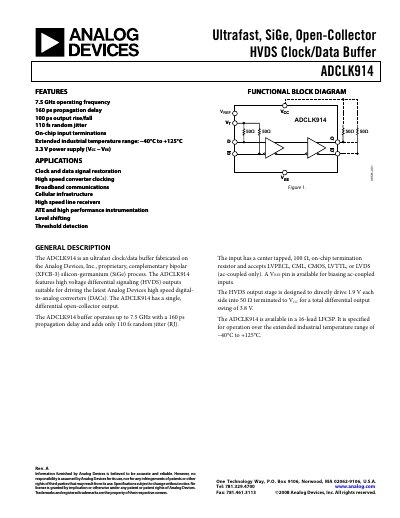
The ADCLK914 is a high‑speed clock and data buffer fabricated on Analog Devices' XFCB‑3 SiGe process. It provides HVDS differential outputs, a single open‑collector output, and supports a 3.3 V supply while operating from –40 °C to +125 °C. The device features on‑chip 50 Ω input terminations and can accept LVPECL, CML, CMOS, LVTTL, or LVDS (ac‑coupled) inputs.
The datasheet includes detailed specifications, pin descriptions, typical performance graphs, layout recommendations, and application circuits for interfacing to high‑speed DACs and other high‑frequency systems. It also provides thermal parameters, absolute maximum ratings, and ordering information for the 16‑lead LFCSP package.
| Operating frequency | 7.5 GHz |
|---|---|
| Propagation delay (typical) | 160 ps |
| Output rise time (typical) | 100 ps |
| Random jitter (RMS) | 110 fs |
| Supply voltage (VCC) | 3.3 V |
| Input voltage range | –0.5 V to VCC+0.5 V |
| Operating temperature range | –40 °C to +125 °C |
The ADCLK914 operates up to 7.5 GHz.
It requires a 3.3 V supply (VCC).
Typical propagation delay is about 160 ps.
The device exhibits 110 fs RMS random jitter.