
Key facts
- Brand
- Philips
- Model
- SOT349-2
- Category
- Other Electronics
- Documents
- 3
- Languages
- EN
- Last added
- 2012-03-22
Start here
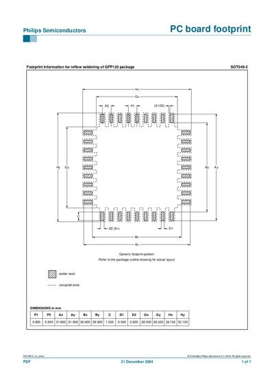
Philips SOT349-2 QFP120 Footprint Datasheet
This document provides the PCB footprint information for reflow soldering of the Philips QFP120 package identified as SOT349-2. It includes the generic footprint pattern, occupied solder land area, and reference dimensions in millimetres.
The layout dimensions are listed in a table and users are instructed to refer to the package outline drawing for the actual layout details. The document is copyrighted by Koninklijke Philips Electronics N.V. (2004).
Philips SOT349-2 specifications
| Pin pitch (Pi) | 0.800 mm |
|---|---|
| Pin pitch (P2) | 0.850 mm |
| Package width (Ax) | 31.900 mm |
| Package height (Ay) | 31.900 mm |
| Solder land width (Bx) | 28.900 mm |
| Solder land height (By) | 28.900 mm |
All Philips SOT349-2 documents by type
Ratings, dimensions and ordering codes, for selection and design work.
Questions answered in these manuals
What package does this footprint apply to?
It applies to the QFP120 package identified as SOT349-2.
Where can I find the actual layout drawing?
Refer to the package outline drawing for the actual layout.
What package does this footprint correspond to?
It is for the QFP120 package SOT349-2.
Where can I find the actual layout drawing?
Refer to the package outline drawing for the actual layout.
What package does this footprint apply to?
It applies to the Philips SOT349-2 QFP120 package.
When was this footprint manual published?
The document was published on 21 December 2004.