
This document provides SOT349-2 PC board printing circuit diagram, including dimensions, coordinates, etc.
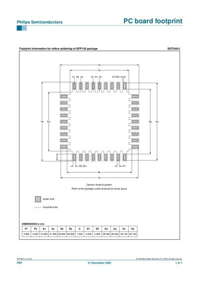
This document provides the PCB footprint information for reflow soldering of the Philips QFP120 package identified as SOT349-2. It includes the generic footprint pattern, occupied solder land area, and reference dimensions in millimetres.
The layout dimensions are listed in a table and users are instructed to refer to the package outline drawing for the actual layout details. The document is copyrighted by Koninklijke Philips Electronics N.V. (2004).
| Pin pitch (Pi) | 0.800 mm |
|---|---|
| Pin pitch (P2) | 0.850 mm |
| Package width (Ax) | 31.900 mm |
| Package height (Ay) | 31.900 mm |
| Solder land width (Bx) | 28.900 mm |
| Solder land height (By) | 28.900 mm |
It applies to the QFP120 package identified as SOT349-2.
Refer to the package outline drawing for the actual layout.