
This document provides information on the PC board footprint and placement accuracy of Philips Semiconductors on February 19, 2001. It includes dimensions and accuracy information for several different package names.
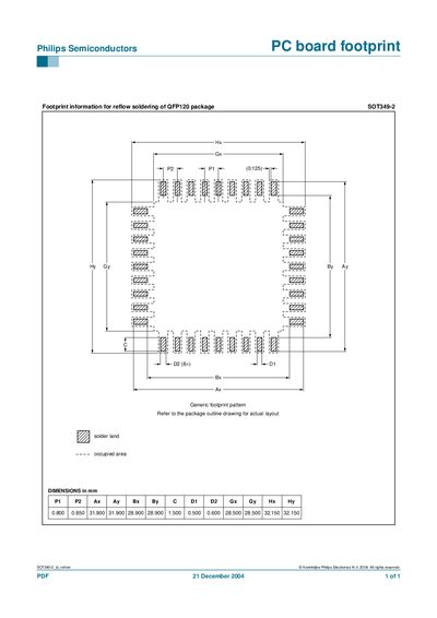
This document provides the printed‑circuit‑board (PC‑board) footprint details for the Philips SOT349-2 QFP120 package, intended for use in reflow soldering processes. It includes pad dimensions, spacing, and the generic footprint pattern.
The generic footprint pattern references the package outline drawing for the exact layout. Dimensions are given in millimetres, with key values such as pad pitch, pad size, and overall package outline size listed in the table.
| Package outline dimensions | 31.900 mm × 31.900 mm |
|---|
It is for the QFP120 package SOT349-2.
Refer to the package outline drawing for the actual layout.
The document was published on 21 December 2004.