
Key facts
- Brand
- Mitsubishi
- Model
- M63814P
- Documents
- 2
- Languages
- EN
- Last added
- 2012-03-21
Start here
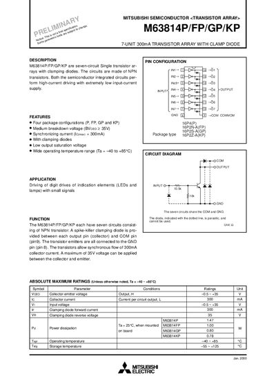
MITSUBISHI M63814P/FP/GP/KP Manual
The M63814 series from Mitsubishi Semiconductor consists of seven NPN transistor circuits with integrated clamping diodes. Each circuit can drive up to 300 mA and operates over a wide temperature range, making it suitable for driving LEDs and small‑signal lamps.
The datasheet provides detailed electrical characteristics, absolute maximum ratings, recommended operating conditions, and thermal derating curves for the four package variants (P, FP, GP, KP). It also includes pin configurations, switching times, and typical performance graphs.
Mitsubishi M63814P specifications
| Collector‑emitter voltage (VCEO) | 0.5 ~ +35 V |
|---|---|
| Collector current per circuit (Ic) | 300 mA |
| Input voltage (VI) | 0.5 ~ +35 V |
| Clamping diode reverse voltage (VR) | 35 V |
| Power dissipation (Pd) – M63814P | 1.47 W |
| Operating temperature range | -40 °C to +85 °C |
| Breakdown voltage (BVcEo) | >35 V |
| Package configurations | P, FP, GP, KP |
All Mitsubishi M63814P documents by type
Ratings, dimensions and ordering codes, for selection and design work.
Questions answered in these manuals
What is the maximum collector‑emitter voltage for the M63814 series?
The series can handle up to 35 V between collector and emitter.
How much current can each circuit output?
Each circuit can output up to 300 mA collector current.
What temperature range can the M63816P/FP/KP operate in?
The device operates from –40 °C up to +85 °C.
What package types are available for the M63816 series?
Package options include 18P4G(P) as well as 20P2E‑A(KP) and 20P2N‑A(FP).