
Key facts
- Brand
- Analog Devices
- Model
- ADP5040
- Industry
- Industrial
- Documents
- 2
- Languages
- EN
- Last added
- 2012-05-04
Start here
Analog Devices ADP5040 Datasheet Handbook
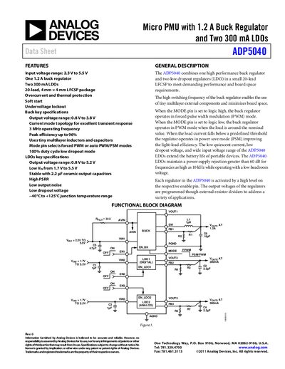
The ADP5040 is a mixed‑signal power management IC that combines a high‑performance 1.2 A buck regulator with two 300 mA low‑dropout regulators (LDOs) in a compact 20‑lead 4 mm × 4 mm LFCSP package. It offers a wide input voltage range, over‑current and thermal protection, soft‑start, and undervoltage lockout, making it suitable for portable and battery‑powered devices.
The document provides detailed specifications such as input and output voltage ranges, switching frequency, efficiency, and PSRR, as well as pin configurations, typical performance curves, recommended external components, and thermal considerations. It also includes a functional block diagram, layout guidelines, and a bill of materials for designers.
Analog Devices ADP5040 specifications
| Input voltage range | 2.3 V to 5.5 V |
|---|---|
| Buck regulator output voltage range | 0.8 V to 3.8 V |
| LDO output voltage range | 0.8 V to 5.2 V |
| Switching frequency | 3 MHz |
| Peak efficiency | up to 96 % |
| Package | 20‑lead 4 mm × 4 mm LFCSP |
All Analog Devices ADP5040 documents by type
Ratings, dimensions and ordering codes, for selection and design work.
Questions answered in these manuals
What is the input voltage range of the ADP5040?
The ADP5040 operates with an input voltage from 2.3 V to 5.5 V.
How many LDO regulators are integrated in the ADP5040?
The device contains two 300 mA low‑dropout regulators.