
Key facts
- Brand
- Toshiba
- Model
- TC7WB66FK
- Industry
- Industrial
- Documents
- 2
- Languages
- EN
- Last added
- 2012-04-01
Start here
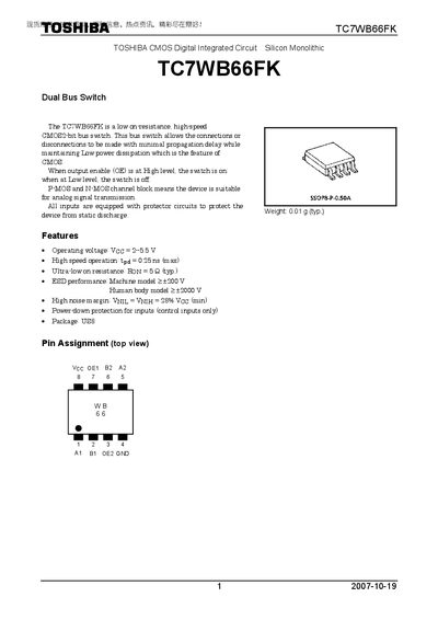
Toshiba TC7WB66FK Dual Bus Switch Datasheet
The TC7WB66FK is a CMOS 2‑bit dual bus switch designed for fast, low‑loss signal routing. It features P‑MOS and N‑MOS channel blocks, built‑in ESD protection, and a compact SSOP8‑P‑0.50A package.
Key specifications include an operating voltage of 2 V to 5.5 V, typical on‑resistance of 5 Ω, propagation delay up to 0.25 ns, and ESD ratings of +200 V (machine model) and +2000 V (human body model). The device is rated for temperatures from –40 °C to 85 °C and is supplied in a 0.01 g package.
Toshiba TC7WB66FK specifications
| Operating voltage (VCC) | 2 V ~ 5.5 V |
|---|---|
| Typical on‑resistance (Ron) | 5 Ω (typ.) |
| Propagation delay (tpd) | 0.25 ns (max) |
| ESD rating (Human Body Model) | +2000 V |
| Weight | 0.01 g (typ.) |
| Power dissipation | 200 mW |
| Switch I/O current | 128 mA |
| Storage temperature range | -65 °C ~ 150 °C |
| Operating temperature range | -40 °C ~ 85 °C |
All Toshiba TC7WB66FK documents by type
Ratings, dimensions and ordering codes, for selection and design work.
Questions answered in these manuals
What is the operating voltage range of the TC7WB66FK?
The device operates with a supply voltage from 2 V to 5.5 V.
What is the typical on‑resistance of the switch?
Typical on‑resistance is 5 Ω.
What is the operating voltage range for the TC7WB66FK?
The device operates with a supply voltage between 2 V and 5.5 V.
What is the typical propagation delay of the TC7WB66FK?
The maximum propagation delay is 0.25 ns.