
TC7WB66FK is a low on-resistance, high-speed CMOS 2-bit bus switch. This bus switch allows the connections or disconnections to be made with minimal propagation delay while maintaining low power dissipation which is the feature of CMOS. When output enable (OE) is at a high level, the switch is on; when at a low level, the switch is off. P-MOS and N-MOS channel block means the device is suitable for analog signal transmission. All inputs are equipped with protector circuits to protect the device from static discharge.
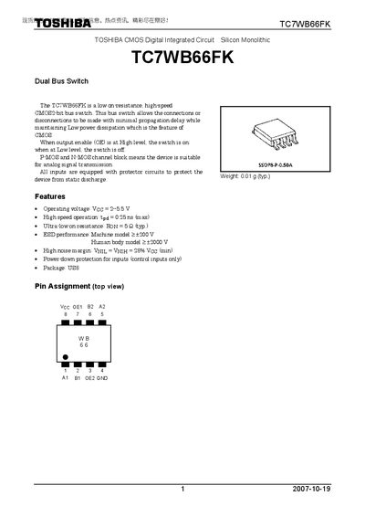
The TC7WB66FK is a CMOS 2‑bit dual bus switch designed for fast, low‑loss signal routing. It features P‑MOS and N‑MOS channel blocks, built‑in ESD protection, and a compact SSOP8‑P‑0.50A package.
Key specifications include an operating voltage of 2 V to 5.5 V, typical on‑resistance of 5 Ω, propagation delay up to 0.25 ns, and ESD ratings of +200 V (machine model) and +2000 V (human body model). The device is rated for temperatures from –40 °C to 85 °C and is supplied in a 0.01 g package.
| Operating voltage (VCC) | 2 V ~ 5.5 V |
|---|---|
| Typical on‑resistance (Ron) | 5 Ω (typ.) |
| Propagation delay (tpd) | 0.25 ns (max) |
| ESD rating (Human Body Model) | +2000 V |
| Weight | 0.01 g (typ.) |
| Power dissipation | 200 mW |
| Switch I/O current | 128 mA |
| Storage temperature range | -65 °C ~ 150 °C |
| Operating temperature range | -40 °C ~ 85 °C |
The device operates with a supply voltage from 2 V to 5.5 V.
Typical on‑resistance is 5 Ω.