
Key facts
- Brand
- Toshiba
- Model
- TC7WG00FC
- Industry
- Industrial
- Documents
- 2
- Languages
- EN
- Last added
- 2012-04-01
Start here
THSHIBA TC7WG00FC Manual(1)
Datasheet 6 pages · 187 KB · EN
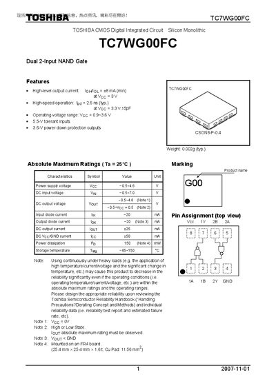
The document provides the full specifications for the Toshiba TC7WGOOFC dual 2‑input NAND gate. It includes features, absolute maximum ratings, DC and AC electrical characteristics, package dimensions, and handling restrictions.
Key sections cover the truth table, operating ranges, propagation delay, input and output current limits, power dissipation, storage temperature, and mechanical drawing of the CSON8‑P‑0.4 package.
Toshiba TC7WG00FC specifications
| High‑level output current (IoH/IoL) | 8 mA (min) |
|---|---|
| Operating voltage range (Vcc) | 0.9 V ~ 3.6 V |
| Propagation delay (tpd) | 2.5 ns (typ.) |
| Power dissipation (Pp) | 150 mW |
| Storage temperature (Tstg) | -65 °C ~ 150 °C |
| Package type | CSON8‑P‑0.4 |
| Weight | 0.002 g (typ.) |
Source: THSHIBA TC7WG00FC Manual(1)
All Toshiba TC7WG00FC documents by type
Datasheet 2
Ratings, dimensions and ordering codes, for selection and design work.
Questions answered in these manuals
What is the operating voltage range of the TC7WGOOFC?
The device operates from 0.9 V to 3.6 V.
What is the maximum power dissipation allowed?
The maximum power dissipation is 150 mW.
What is the operating voltage range for the TC7WGOOFC?
The device operates from 0.9 V to 3.6 V supply voltage.
What is the minimum high‑level output current?
The high‑level output current is at least 8 mA when Vcc is 3 V.