
Key facts
- Brand
- Toshiba
- Model
- TC7SH32FU
- Industry
- Industrial
- Documents
- 2
- Languages
- EN
- Last added
- 2012-04-01
Start here
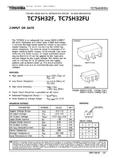
THSHIBA TC7SH32F TC7SH32FU Manual
The TC7SH32F/FU is a high‑speed CMOS 2‑input OR gate designed for low power dissipation and high noise immunity. It operates over a wide supply range and includes input protection for 0‑7 V signals, making it suitable for interfacing 5 V to 3 V systems.
Key specifications include a supply voltage range of –0.5 V to 7.0 V, typical power dissipation of 200 mW, and operation in temperatures from –40 °C to 85 °C. The device is offered in SSOP5‑P‑0.95 and SSOP5‑P‑0.65 packages with typical weights of 0.016 g and 0.006 g respectively.
Toshiba TC7SH32FU specifications
| Input Voltage (VIN) | -0.5~7.0 V |
|---|---|
| Output Voltage (VOUT) | -0.5~Vcc+0.5 V |
| Power Dissipation (PD) | 200 mW |
| Storage Temperature (Tstg) | -65~150 °C |
| Lead Temperature (TL, 10 s) | 260 °C |
All Toshiba TC7SH32FU documents by type
Ratings, dimensions and ordering codes, for selection and design work.
Questions answered in these manuals
What is the typical power dissipation of the TC7SH32F/FU?
Typical power dissipation is 200 mW.
What is the operating temperature range of the device?
The device can operate from –40 °C to 85 °C.
Which package options are available for this IC?
It is offered in SSOP5‑P‑0.95 and SSOP5‑P‑0.65 packages.
What is the typical power dissipation of the TC7SH32F/FU?
Typical power dissipation is 200 mW.