
Key facts
- Brand
- Toshiba
- Model
- TC7SH14FU
- Industry
- Industrial
- Documents
- 2
- Languages
- EN
- Last added
- 2012-04-01
Start here
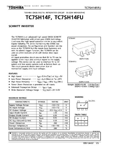
THSHIBA TC7SH14F TC7SH14FU Manual
This document describes the Toshiba TC7SH14F/FU CMOS Schmitt inverter, highlighting its high‑speed operation, low power dissipation, and built‑in input protection. It includes a feature list, maximum ratings, recommended operating conditions, and detailed electrical characteristics.
The datasheet also provides pin assignment diagrams, package outline drawings for the SSOP5‑P‑0.95 and SSOP5‑P‑0.65A packages, and typical values such as propagation delay, power dissipation, and operating temperature range.
Toshiba TC7SH14FU specifications
| Supply voltage range | 2.0 V to 5.5 V |
|---|---|
| Power dissipation | 200 mW |
| Operating temperature range | -40 °C to 85 °C |
| Input diode current (leakage) | -20 mA |
| Package weight (SSOP5‑P‑0.95) | 0.016 g (Typ.) |
| Input capacitance | 10 pF |
All Toshiba TC7SH14FU documents by type
Ratings, dimensions and ordering codes, for selection and design work.
Questions answered in these manuals
What supply voltage range does the TC7SH14F/FU support?
It operates from 2.0 V up to 5.5 V.
How much power can the TC7SH14F/FU dissipate?
The device can dissipate up to 200 mW.
What supply voltage range can the device operate in?
It operates from 2.0 V to 5.5 V, with absolute ratings of –0.5 V to 7.0 V.
Does the IC provide input protection?
Yes, it includes power‑down protection on all inputs and can tolerate up to 7 V on the input pins.