
SN74AC11 series is a three-input AND gate. The inputs can accept voltages up to 6V, and the VCC supply voltage range is 2V to 6V. The series has a maximum delay time of 7.5ns and can operate normally at 5V. This datasheet provides information on the pinout, package type, function table, etc. of the SN74AC11 series.
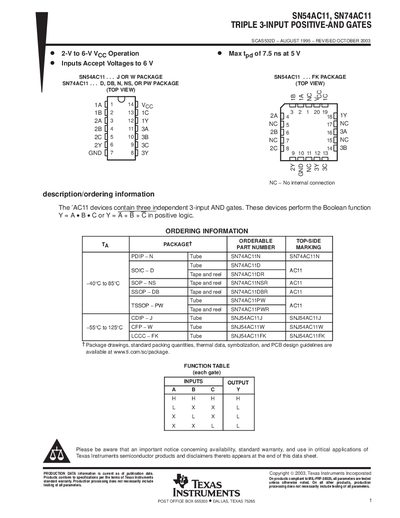
The SN54AC11 and SN74AC11 are triple 3‑input positive‑AND gate devices that implement the Boolean function Y = A·B·C in positive logic. The data sheet provides functional tables, absolute maximum ratings, recommended operating conditions, and detailed electrical characteristics for each supported package.
The document also lists all available package types (PDIP, SOIC, SSOP, TSSOP, etc.), their thermal impedance, and mechanical dimensions, along with ordering part numbers and RoHS compliance information.
| Supply voltage range (VCC) | 2 V to 6 V |
|---|---|
| Output voltage range | -0.5 V to VCC + 0.5 V |
| Operating temperature range (PDIP, SOIC, etc.) | -55 °C to 125 °C |
For PDIP, SOIC, and similar packages the range is –55 °C to 125 °C; for SSOP, TSSOP and other surface‑mount packages it is –40 °C to 85 °C.
Available packages include PDIP (N), SOIC (D), SSOP (DB), TSSOP (PW), CDIP (J), CFP (W), and LOCC (FK), each with corresponding part numbers.