
Key facts
- Brand
- Analog Devices
- Model
- AD8099
- Industry
- Industrial
- Documents
- 2
- Languages
- EN
- Last added
- 2012-05-02
Start here
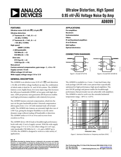
Analog Devices AD8099 Handbook Datasheet
The AD8099 op‑amp delivers ultralow voltage‑noise (0.95 nV/√Hz) and ultralow distortion (‑92 dBc @10 MHz) with a high gain‑bandwidth product of 3.8 GHz. It features a new linear, low‑noise input stage, external compensation for gains from +2 to +10, and a very high slew rate (up to 1350 V/µs). The device operates from a wide supply range (5 V‑12 V) and draws only about 15 mA quiescent current.
Designed for 16‑bit and 18‑bit systems, the AD8099 is suited for pre‑amplifiers, receivers, instrumentation, filters, A‑to‑D drivers, DAC buffers, and optical electronics. It is available in 8‑lead SOIC‑ED and 8‑lead CSP packages with a temperature range of –40 °C to +125 °C.
Analog Devices AD8099 specifications
| Voltage Noise | 0.95 nV/√Hz |
|---|---|
| Gain‑Bandwidth Product | 3.8 GHz |
| Slew Rate (G = +2) | 475 V/µs |
| Supply Voltage Range | 5 V to 12 V |
All Analog Devices AD8099 documents by type
Ratings, dimensions and ordering codes, for selection and design work.
Questions answered in these manuals
What is the maximum supply voltage rating?
The absolute maximum supply voltage is 12.6 V.
What is the input offset voltage range?
The input offset voltage is specified as 0.1 mV to 0.5 mV.
What is the typical settling time of the AD8099?
The AD8099 settles to 0.1 % in 18 ns.
What is the maximum supply voltage rating for the AD8099?
The device is rated for a maximum supply voltage of 12.6 V.