
The AD8099 is an ultralow distortion, high-speed operational amplifier with a voltage noise of 0.95 nV/√Hz and a current noise of 2.6 pA/√Hz. It features ultralow distortion, with the second harmonic at -92 dB @ 10 MHz and the third harmonic at -105 dB @ 10 MHz. The op amp has a high speed with a gain bandwidth product (GBWP) of 3.8 GHz and a -3 dB bandwidth of 700 MHz (G = +2) and 550 MHz (G = +10). It has a slew rate of 475 V/µs (G = +2) and 1350 V/µs (G = +10). It has a new pinout and allows for custom external compensation with a gain range of -1, +2 to +10. It is suitable for applications such as pre-amplifiers, receivers, instrumentation, filters, A-to-D drivers, DAC buffers, and optical electronics.
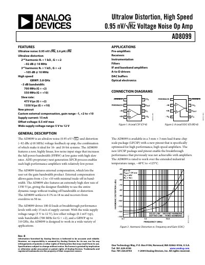
The AD8099 op‑amp delivers ultralow voltage‑noise (0.95 nV/√Hz) and ultralow distortion (‑92 dBc @10 MHz) with a high gain‑bandwidth product of 3.8 GHz. It features a new linear, low‑noise input stage, external compensation for gains from +2 to +10, and a very high slew rate (up to 1350 V/µs). The device operates from a wide supply range (5 V‑12 V) and draws only about 15 mA quiescent current.
Designed for 16‑bit and 18‑bit systems, the AD8099 is suited for pre‑amplifiers, receivers, instrumentation, filters, A‑to‑D drivers, DAC buffers, and optical electronics. It is available in 8‑lead SOIC‑ED and 8‑lead CSP packages with a temperature range of –40 °C to +125 °C.
| Voltage Noise | 0.95 nV/√Hz |
|---|---|
| Gain‑Bandwidth Product | 3.8 GHz |
| Slew Rate (G = +2) | 475 V/µs |
| Supply Voltage Range | 5 V to 12 V |
The absolute maximum supply voltage is 12.6 V.
The input offset voltage is specified as 0.1 mV to 0.5 mV.