
This document describes the features and characteristics of the AD8099 Rev. B, an ultralow distortion, high-speed 0.95 nV/√Hz voltage noise operational amplifier.
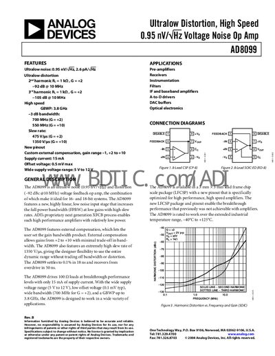
The AD8099 is a voltage‑feedback operational amplifier designed for 16‑ and 18‑bit systems. It features an ultralow noise floor of 0.95 nV/√Hz, harmonic distortion better than –92 dBc at 10 MHz, and a gain‑bandwidth product of 3.8 GHz. The device offers a new pinout, external compensation for gains from +2 to +10, and a very high slew rate of up to 1350 V/µs.
Typical applications include pre‑amplifiers, receivers, instrumentation, filters, DAC buffers, and optical electronics. The AD8099 operates from a wide supply range (5 V‑12 V), draws only 15 mA, and is rated for an industrial temperature range of –40 °C to +125 °C.
| Voltage Noise (100 kHz) | 0.95 nV/√Hz |
|---|---|
| Gain‑Bandwidth Product | 3.8 GHz |
| Slew Rate (G=+10) | 1350 V/µs |
| Supply Current | 15 mA |
| Supply Voltage Range | 5 V to 12 V |
| Operating Temperature Range | –40 °C to +125 °C |
The AD8099 settles to 0.1 % in 18 ns.
The device is rated for a maximum supply voltage of 12.6 V.
Typical input offset voltage is 0.1 mV.