
Key facts
- Brand
- Analog Devices
- Model
- AD561
- Industry
- Industrial
- Documents
- 2
- Languages
- EN
- Last added
- 2012-05-02
Start here
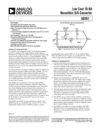
Analog Devices AD561 Low Cost 10-Bit Monolithic D/A Converter Handbook
The AD561 is an integrated‑circuit 10‑bit digital‑to‑analog converter that combines a high‑stability buried Zener reference, laser‑trimmed resistor network, and fast current‑steering switches on a single monolithic chip. It offers true 10‑bit resolution, monotonic performance over the full temperature range, and optional MIL‑STD‑883‑compliant packages.
The device provides unipolar output currents of up to 2.4 mA, a compliance voltage from –3 V to +10 V (guaranteed –2 V to +10 V), and a typical settling time of less than 250 ns to 1/2 LSB. Power supplies from +4.5 V to +16.5 V (positive) and –10.8 V to –16.5 V (negative) are supported, with temperature grades ranging from 0 °C to +70 °C (J/K) and –55 °C to +125 °C (S/T).
Analog Devices AD561 specifications
| Resolution | 10 bits |
|---|---|
| Accuracy (max error) | 1/4 LSB (0.025 % of FS) for K/T grades |
| Compliance Voltage | –3 V to +10 V (typ), –2 V to +10 V (guaranteed) |
| Settling Time (to 1/2 LSB) | < 250 ns |
| Power Supply Range (positive) | +4.5 V to +16.5 V |
| Power Supply Range (negative) | –10.8 V to –16.5 V |
Source: Analog Devices AD561 Low Cost 10-Bit Monolithic D/A Converter Handbook
All Analog Devices AD561 documents by type
Ratings, dimensions and ordering codes, for selection and design work.
Questions answered in these manuals
What is the settling time of the AD561?
The typical settling time to 1/2 LSB is less than 250 ns for the worst‑case transition.
From: Analog Devices AD561 Low Cost 10-Bit Monolithic D/A Converter Handbook
What is the output voltage compliance range?
The AD561 provides a typical compliance range of –3 V to +10 V and is guaranteed to be –2 V to +10 V with VEE = –15 V.
From: Analog Devices AD561 Low Cost 10-Bit Monolithic D/A Converter Handbook
What is the settling time of the AD561?
The AD561 settles to ½ LSB in about 250 ns for the worst‑case code transition.
What is the output voltage compliance range of the AD561?
The device provides an output voltage compliance from –2 V to +10 V.