
The AD561 is an integrated circuit 10-bit digital-to-analog converter combined with a high stability voltage reference fabricated on a single monolithic chip.
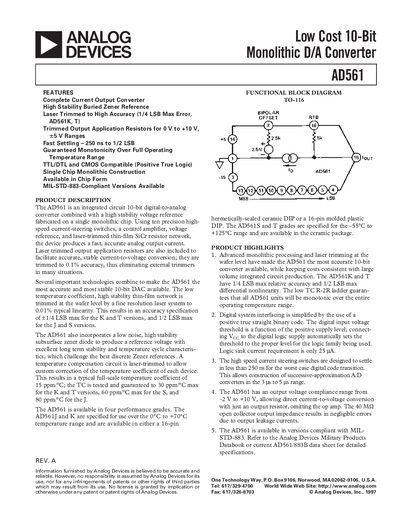
The AD561 is an integrated‑circuit 10‑bit digital‑to‑analog converter that combines a high‑stability buried Zener reference, laser‑trimmed resistor network, and fast current‑steering switches on a single monolithic chip. It offers true 10‑bit resolution, monotonic performance over the full temperature range, and optional MIL‑STD‑883‑compliant packages.
The device provides unipolar output currents of up to 2.4 mA, a compliance voltage from –3 V to +10 V (guaranteed –2 V to +10 V), and a typical settling time of less than 250 ns to 1/2 LSB. Power supplies from +4.5 V to +16.5 V (positive) and –10.8 V to –16.5 V (negative) are supported, with temperature grades ranging from 0 °C to +70 °C (J/K) and –55 °C to +125 °C (S/T).
| Resolution | 10 bits |
|---|---|
| Accuracy (max error) | 1/4 LSB (0.025 % of FS) for K/T grades |
| Compliance Voltage | –3 V to +10 V (typ), –2 V to +10 V (guaranteed) |
| Settling Time (to 1/2 LSB) | < 250 ns |
| Power Supply Range (positive) | +4.5 V to +16.5 V |
| Power Supply Range (negative) | –10.8 V to –16.5 V |
The typical settling time to 1/2 LSB is less than 250 ns for the worst‑case transition.
The AD561 provides a typical compliance range of –3 V to +10 V and is guaranteed to be –2 V to +10 V with VEE = –15 V.
AD561J and AD561K operate from 0 °C to +70 °C, while AD561S and AD561T operate from –55 °C to +125 °C.
All standard positive‑supply logic families (TTL, DTL, CMOS) interface easily with the AD561.