
Key facts
- Brand
- Toshiba
- Model
- TC7SA00FU
- Industry
- Industrial
- Documents
- 3
- Languages
- EN
- Last added
- 2012-04-01
Start here
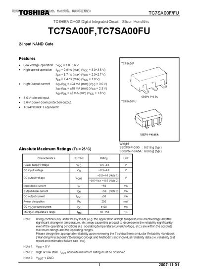
THSHIBA TC7SA00F TC7SA00FU Manual
The TC7SA00F/FU is a CMOS 2‑input NAND gate designed for low‑voltage operation (1.8‑3.6 V) and high‑speed switching. It offers typical propagation delays of 2.8 ns at 3.0‑3.6 V supply and output currents up to 24 mA.
The datasheet provides absolute maximum ratings, DC and AC electrical characteristics, dynamic switching behavior, package dimensions for SSOP5‑P‑0.95 and SSOP5‑P‑0.65A, and usage restrictions for safety‑critical applications.
Toshiba TC7SA00FU specifications
| Propagation delay (tpd) | 2.8 ns max (VCC 3.0‑3.6 V) |
|---|---|
| Output high current (IOH) | 24 mA min (VCC 3.0 V) |
| Operating temperature range | -40 °C – 85 °C |
| Storage temperature range | -65 °C – 150 °C |
| Package weight (SSOP5‑P‑0.95) | 0.016 g (typ.) |
All Toshiba TC7SA00FU documents by type
Ratings, dimensions and ordering codes, for selection and design work.
Questions answered in these manuals
What is the maximum propagation delay of the device?
The typical maximum propagation delay is 2.8 ns when VCC is between 3.0 V and 3.6 V.
What is the operating voltage range for the TC7SA00F/FU?
The device operates from 1.8 V to 3.6 V.
What is the maximum propagation delay of the IC?
The maximum propagation delay is 2.8 ns when Vcc is between 3.0 V and 3.6 V.
What is the recommended power supply voltage range?
The device operates with a supply voltage (Vcc) from 1.8 V to 3.6 V.
From: Toshiba TC7SA00F/TC7SA00FU 2-Input NAND Gate Datasheet
What is the maximum propagation delay?
The maximum propagation delay is 2.8 ns when Vcc is between 3.0 V and 3.6 V.
From: Toshiba TC7SA00F/TC7SA00FU 2-Input NAND Gate Datasheet