
TC7SA00F/FU is a 2-input NAND gate chip produced by Toshiba. Its features are low voltage operation, high speed operation, high output current, 3.6V tolerant input, and 3.6V power down protection output.
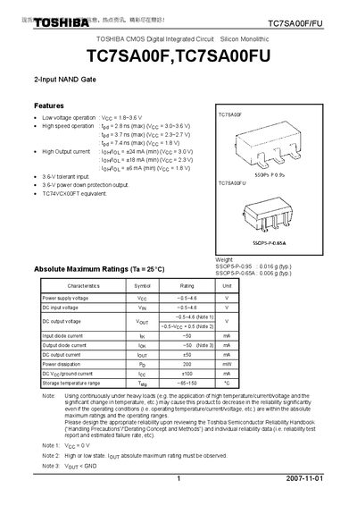
The TC7SA00F/FU is a CMOS 2‑input NAND gate designed for low‑voltage operation (1.8‑3.6 V) and high‑speed switching. It offers typical propagation delays of 2.8 ns at 3.0‑3.6 V supply and output currents up to 24 mA.
The datasheet provides absolute maximum ratings, DC and AC electrical characteristics, dynamic switching behavior, package dimensions for SSOP5‑P‑0.95 and SSOP5‑P‑0.65A, and usage restrictions for safety‑critical applications.
| Propagation delay (tpd) | 2.8 ns max (VCC 3.0‑3.6 V) |
|---|---|
| Output high current (IOH) | 24 mA min (VCC 3.0 V) |
| Operating temperature range | -40 °C – 85 °C |
| Storage temperature range | -65 °C – 150 °C |
| Package weight (SSOP5‑P‑0.95) | 0.016 g (typ.) |
The typical maximum propagation delay is 2.8 ns when VCC is between 3.0 V and 3.6 V.