
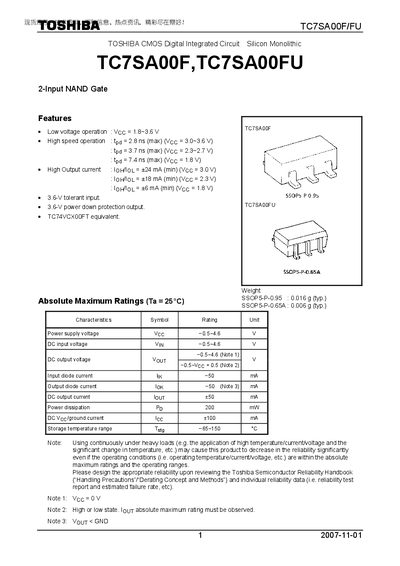
The TC7SA00F/FU is a CMOS 2‑input NAND gate offered in SSOP5 packages. It operates from 1.8 V to 3.6 V, provides high output current (up to 24 mA) and fast propagation delays as low as 2.8 ns at typical supply voltages.
The device is intended for general electronics applications such as computers, office equipment, and industrial robotics. It must not be used in safety‑critical or high‑reliability systems (e.g., medical, aerospace, traffic control) and must comply with all applicable safety and environmental regulations.
| Supply voltage (Vcc) | 1.8 V – 3.6 V |
|---|---|
| Propagation delay (tpd) | 2.8 ns (max) at Vcc = 3.0‑3.6 V |
| Output current (IoH/IoL) | 24 mA (min) at Vcc = 3.0 V |
| Storage temperature range | -65 °C – 150 °C |
| Package weight (SSOP5‑P‑0.95) | 0.016 g (typ.) |
The device operates from 1.8 V to 3.6 V.
The maximum propagation delay is 2.8 ns when Vcc is between 3.0 V and 3.6 V.