
Key facts
- Brand
- Samsung
- Model
- K4S280432M
- Industry
- Industrial
- Documents
- 2
- Languages
- EN
- Last added
- 2012-04-01
Start here
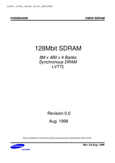
Samsung K4S280432M CMOS SDRAM Datasheet
This document describes the Samsung K4S280432M 128 Mbit CMOS SDRAM, a synchronous DRAM organized as 8M × 4 bit × 4 banks. It includes features such as JEDEC‑standard 3.3 V operation, selectable CAS latency, and programmable burst lengths.
The datasheet contains ordering information, functional block diagrams, pin layouts, absolute maximum ratings, DC and AC operating conditions, IBIS specifications, and a simplified truth table for command timing.
Samsung K4S280432M specifications
| Capacity | 128 Mbit |
|---|---|
| Organization | 8M × 4 bit × 4 banks |
| Supply voltage (Vob, VDDQ) | 3.0 V min / 3.3 V typ / 3.6 V max |
| CAS latency options | 2 or 3 |
| Burst length options | 1, 2, 4, or 8 |
| Maximum operating frequency | 125 MHz (CL=3) |
| Storage temperature range | -55 °C to +150 °C |
All Samsung K4S280432M documents by type
Ratings, dimensions and ordering codes, for selection and design work.
Questions answered in these manuals
What is the supply voltage range for the K4S280432M?
The device operates with a supply voltage of 3.0 V minimum, 3.3 V typical, and 3.6 V maximum.
What CAS latency values can be selected?
The SDRAM supports CAS latency values of 2 or 3.
What is the supply voltage range for the K4S280432M?
The device operates from 3.0 V (minimum) to 3.6 V (maximum) with a typical voltage of 3.3 V.
Which CAS latency values does the K4S280432M support?
The SDRAM supports CAS latency values of 2 and 3.