
Key facts
- Brand
- Samsung
- Model
- K4S280432B
- Industry
- Industrial
- Documents
- 2
- Languages
- EN
- Last added
- 2012-04-01
Start here
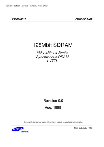
Samsung K4S280432B CMOS SDRAM Datasheet
Datasheet 10 pages · 128 KB · EN
This document describes the Samsung K4S280432B 128‑Mbit CMOS SDRAM. It includes the memory organization, functional block diagram, pin layout, and detailed electrical characteristics for designers.
Key sections cover absolute maximum ratings, DC and AC operating conditions, IBIS specifications, and command timing tables, allowing engineers to integrate the part into high‑performance memory systems.
Samsung K4S280432B specifications
| Memory density | 128 Mbit |
|---|---|
| Organization | 8M x 4‑bit x 4 banks |
| Supply voltage (Vop, Vopa) | 3.0 V min / 3.3 V typ / 3.6 V max |
| Storage temperature range | -55 °C to +150 °C |
| Power dissipation | 1 W |
| Package | 54‑pin TSOP |
All Samsung K4S280432B documents by type
Datasheet 2
Ratings, dimensions and ordering codes, for selection and design work.
Questions answered in these manuals
What is the supply voltage range for the K4S280432B?
The device operates with a supply voltage of 3.0 V minimum, 3.3 V typical, and 3.6 V maximum.
How many banks does the K4S280432B have?
It is organized into four banks.
What supply voltage range does the K4S280432B require?
The device operates from 3.0 V (minimum) to 3.6 V (maximum) with a typical value of 3.3 V.
What is the maximum clock frequency supported?
Up to 133 MHz when configured with CAS latency 3.