
Key facts
- Brand
- Samsung
- Model
- ONENAND1G
- Industry
- Industrial
- Documents
- 2
- Languages
- EN
- Last added
- 2012-06-11
Start here
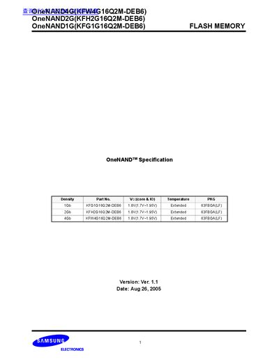
SAMSUNG ELECTRONICS OneNAND4G(KFW4G16Q2M-DEB6) OneNAND2G(KFH2G16Q2M-DEB6) OneNAND1G(KFG1G16Q2M-DEB6) FLASH MEMORY handbook
This document is a specification sheet for the Samsung OneNAND Flash memory product family, covering densities of 1Gb, 2Gb, and 4Gb. It details the device architecture, which integrates a NAND Flash array with a NOR Flash interface, internal buffers, and error correction capabilities. The document outlines various product features such as multiple reset modes, multi-block erase, and low power dissipation options for Single, DDP, and QDP configurations.
Read onlineSamsung ONENAND1G specifications
| Page Size | (2K+64)B |
|---|---|
| Block Size | (128K+4K)B |
| Maximum Clock Frequency | 66MHz |
| Asynchronous Random Read Access Time | 76ns |
| Endurance | 100K Program/Erase Cycles |
| Data Retention | 10 Years |
| Package Type | 63ball FBGA |
All Samsung ONENAND1G documents by type
Ratings, dimensions and ordering codes, for selection and design work.
Questions answered in these manuals
What is the operating temperature range for the Extended temperature version?
The Extended temperature range is -30°C to 85°C.
Does the device include on-chip error correction?
Yes, the device includes Internal 2bit EDC / 1bit ECC.
What is the maximum host-driven clock frequency for synchronous reads?
The device supports a maximum clock frequency of 54MHz for synchronous read operations.
How many program and erase cycles can this memory endure?
This flash memory is rated for an endurance of 100K Program/Erase Cycles.