
Key facts
- Brand
- Samsung
- Model
- ONENAND256
- Industry
- Industrial
- Documents
- 2
- Languages
- EN
- Last added
- 2012-06-11
Start here
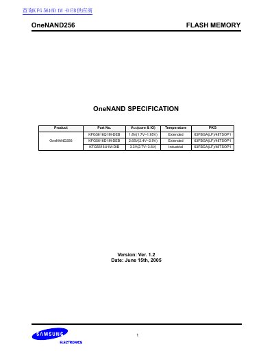
Samsung OneNAND256 Flash Memory Datasheet
Datasheet 93 pages · 1.2 MB · EN
This document is a technical datasheet for the Samsung OneNAND256 Flash Memory, a single-die chip combining a standard NOR Flash interface with a NAND Flash array and 3KB internal BufferRAM. The device supports operating clock frequencies up to 54MHz and offers multiple voltage options (1.8V, 2.65V, and 3.3V) depending on the specific part number.
Read onlineSamsung ONENAND256 specifications
| Design Technology | 0.12µm |
|---|---|
| Host Interface | 16bit |
| Internal BufferRAM | 3K Bytes |
| Page Size | (1K+32)bytes |
| Block Size | (64K+2K)bytes |
| Clock Frequency | up to 54MHz |
| Asynchronous Random Read Access time | 76ns |
| Endurance | 100K Program/Erase Cycles |
| Data Retention | 10 Years |
All Samsung ONENAND256 documents by type
Datasheet 1
Ratings, dimensions and ordering codes, for selection and design work.
Questions answered in these manuals
What is the maximum operating clock frequency for this device?
The operating clock frequency is up to 54MHz.
What is the access time for asynchronous random reads?
The access time for asynchronous random reads is 76ns.