
Key facts
- Brand
- Toshiba
- Model
- TC7WG08FU
- Industry
- Industrial
- Documents
- 2
- Languages
- EN
- Last added
- 2012-04-01
Start here
THSHIBA TC7WG08FU TC7WG08FK Manual
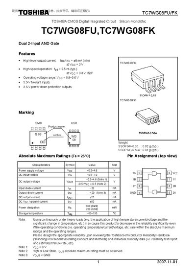
The TC7WGO8FU/TC7WG08FK is a Toshiba CMOS dual 2‑input AND gate offering high‑level output current of up to +8 mA and a typical propagation delay of 2.5 ns at 3.3 V supply. It operates over a wide voltage range (0.9‑3.6 V), features 5.5‑V tolerant inputs and 3.6‑V power‑down protection on the outputs, and is supplied in a compact SSOP‑8 package.
The device is intended for general electronics applications such as computers, office equipment, measuring instruments and industrial robotics. Users must observe the absolute maximum ratings and reliability guidelines provided in Toshiba’s Semiconductor Reliability Handbook to ensure safe and reliable designs.
Toshiba TC7WG08FU specifications
| High‑level output current | +8 mA at VCC=3.3 V |
|---|---|
| Propagation delay (tpd) | 2.5 ns typ. |
| Operating voltage range (VCC) | 0.9 V ~ 3.6 V |
| Input tolerance | 5.5‑V tolerant inputs |
| Power‑down protection output voltage | 3.6‑V |
| Package type | SSOP8‑P‑0.65 (0.02 g typ.) |
| Absolute maximum input voltage | -0.5 V ~ 7.0 V |
All Toshiba TC7WG08FU documents by type
Ratings, dimensions and ordering codes, for selection and design work.
Questions answered in these manuals
What is the typical propagation delay of the TC7WGO8FU?
The typical propagation delay is 2.5 ns.
What voltage range can the device operate in?
It operates from 0.9 V to 3.6 V supply.
What is the operating voltage range for the TC7WGO8FU/FK devices?
The devices operate with a supply voltage from 0.9 V to 3.6 V.
What is the typical high‑level output current of these AND gates?
The typical high‑level output current is +8 mA.