
Key facts
- Brand
- Toshiba
- Model
- TC7WG08FC
- Industry
- Industrial
- Documents
- 2
- Languages
- EN
- Last added
- 2012-04-01
Start here
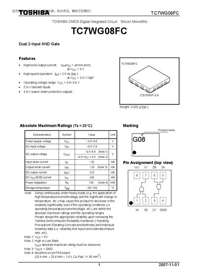
Toshiba TC7WG08FC Dual 2-Input AND Gate Datasheet
Datasheet 6 pages · 187 KB · EN
The TC7WG08FC is a dual 2‑input AND gate semiconductor device from Toshiba. The document provides detailed electrical characteristics, package information, and usage restrictions for designers.
Key data include operating voltage ranges, output current capabilities, propagation delay, and power dissipation limits, along with recommended handling and reliability guidelines.
Toshiba TC7WG08FC specifications
| Operating voltage range | 0.9–3.6 V |
|---|---|
| High‑level output current | ≥8 mA (min) at Vcc = 3 V |
| Propagation delay (tpd) | 2.5 ns typ. |
| Power dissipation | 150 mW |
| Storage temperature | -65 °C to 150 °C |
| Package dimensions (CSON8‑P‑0.4) | 1.35 mm × 0.05 mm |
All Toshiba TC7WG08FC documents by type
Datasheet 2
Ratings, dimensions and ordering codes, for selection and design work.
Questions answered in these manuals
What is the maximum operating voltage for the TC7WG08FC?
The device can operate up to 3.6 V (Vcc = 0.9–3.6 V).
What is the typical propagation delay of the gate?
Typical propagation delay is 2.5 ns.