
TC7WG08FU/FK is a dual 2-input AND gate produced by Toshiba Corporation. It has features such as high-level output current, high-speed operation, wide operating voltage range, input tolerance of 5.5 V, and output undervoltage protection of 3.6 V.
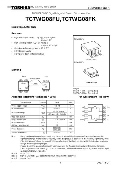
The Toshiba TC7WGO8FU and TC7WG08FK are dual 2‑input AND gate ICs offered in SSOP‑8 packages. The datasheet provides detailed electrical characteristics, absolute maximum ratings, and recommended operating ranges for reliable circuit design.
Key sections include features, pin assignment, logic truth table, AC and DC characteristics, package dimensions, and restrictions on product use. The document also contains reliability guidance and handling precautions for designers.
| High‑level output current | +8 mA |
|---|---|
| Propagation delay (tpd) | 2.5 ns (typ.) |
| Operating voltage range (VCC) | 0.9 V ~ 3.6 V |
| Package dimensions (SSOP8‑P‑0.65) | 2.94 mm × 0.65 mm |
| Typical weight (SSOP8‑P‑0.65) | 0.02 g |
| Power dissipation (US8) | 200 mW |
The devices operate with a supply voltage from 0.9 V to 3.6 V.
The typical high‑level output current is +8 mA.
The typical propagation delay is 2.5 ns.
The SSOP8‑P‑0.65 package measures approximately 2.94 mm by 0.65 mm.