
Key facts
- Brand
- Samsung
- Model
- K4S513233F
- Documents
- 2
- Languages
- EN
- Last added
- 2012-04-01
Start here
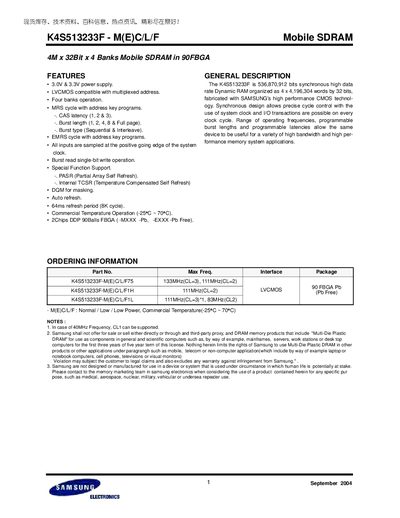
Samsung K4S513233F Mobile SDRAM Datasheet
The document describes the K4S513233F Mobile SDRAM, a 4‑bank, 4 M × 32‑bit device packaged in a 90‑ball FBGA. It lists features such as 3.0 V/3.3 V operation, programmable burst lengths, and partial array self‑refresh. Detailed pin‑out diagrams, package dimensions, and electrical characteristics are included.
Operating specifications cover absolute maximum ratings, recommended DC and AC conditions, timing parameters, and the required power‑up sequence. The datasheet also provides ordering information, model suffix meanings, and notes on usage restrictions.
Samsung K4S513233F specifications
| Supply Voltage | 3.0 V – 3.3 V |
|---|---|
| Package | 90‑ball FBGA |
| Maximum Operating Frequency | 133 MHz (CL5) |
| Operating Temperature Range | -25 °C to 70 °C (commercial) |
| Refresh Period | 64 ms (8K cycles) |
| Maximum Pin Voltage | -1.0 V to +46 V |
All Samsung K4S513233F documents by type
Ratings, dimensions and ordering codes, for selection and design work.
Questions answered in these manuals
What are the absolute maximum voltage ratings for the device pins?
Pins may tolerate voltages from –1.0 V to +46 V relative to VSS.
What package type is used for the K4S513233F?
The chip is supplied in a 90‑ball FBGA package.
What is the maximum operating frequency for the K4S513233F-M(E)C/L/F?
The part is specified for up to 133 MHz operation.
What package type does the K4S513233F use?
It is supplied in a 90‑ball FBGA package.