
The document describes the features and characteristics of TOSHIBA CMOS Digital Integrated Circuit Silicon Monolithic TC7WG00FC, including high-level output current, high-speed operation, operating voltage range, 5.5V tolerant inputs, and 3.6V power down protection outputs.
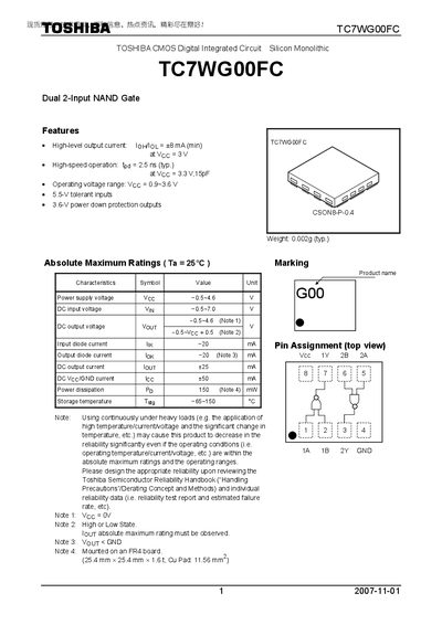
The TC7WGOOFC is a Toshiba CMOS dual 2‑input NAND gate designed for low‑voltage operation (0.9 V ~ 3.6 V). It offers high‑level output current of at least 8 mA at 3 V, high‑speed propagation (2.5 ns typ. at 3.3 V, 15 pF), and includes built‑in power‑down protection.
The document lists detailed DC and AC electrical characteristics, package dimensions (CSON8‑P‑0.4, 1.35 × 0.05 mm, 0.002 g), and strict usage restrictions, emphasizing that the device must not be used in safety‑critical or high‑reliability applications such as medical, aerospace, or transportation equipment.
| High‑level output current (IoH/loL) | ≥8 mA (min) at Vcc = 3 V |
|---|---|
| Propagation delay (tpd) | 2.5 ns (typ.) at Vcc = 3.3 V, 15 pF |
| Operating voltage range | 0.9 V ~ 3.6 V |
| Input diode current | -20 mA |
| Power dissipation | 150 mW (typ.) |
| Storage temperature | -65 °C ~ 150 °C |
| Package size (CSON8‑P‑0.4) | 1.35 mm × 0.05 mm (typ.) |
| Weight | 0.002 g (typ.) |
The device operates from 0.9 V to 3.6 V supply voltage.
The high‑level output current is at least 8 mA when Vcc is 3 V.
The component can be stored between –65 °C and 150 °C.