
Key facts
- Brand
- STMicroelectronics
- Model
- STP2NK60Z
- Industry
- Industrial
- Documents
- 2
- Languages
- EN
- Last added
- 2012-08-07
Start here
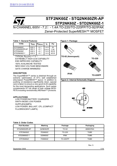
ST STF2NK60Z/STQ2NK60ZR-AP/STP2NK60Z/STD2NK60Z-1 handbook
This document provides technical specifications for the STF2NK60Z, STQ2NK60ZR-AP, STP2NK60Z, and STD2NK60Z-1 N-channel MOSFETs. These devices utilize ST's SuperMESH™ layout technology to achieve low on-resistance while maintaining high dv/dt capability for demanding applications.
Read onlineSTMicroelectronics STP2NK60Z specifications
| Drain‑Source Voltage (VDS) | 600 V |
|---|---|
| Total Power Dissipation (PD) at 25 °C | 45 W |
| Avalanche Current (IAval) | 14 A |
Source: STMicroelectronics STF2NK60Z / STQ2NK60ZR-AP / STP2NK60Z / STD2NK60Z-1 Datasheet
All STMicroelectronics STP2NK60Z documents by type
Ratings, dimensions and ordering codes, for selection and design work.
Questions answered in these manuals
Do these devices include built-in protection?
Yes, they feature integrated back-to-back Zener diodes to enhance ESD capability and safely absorb voltage transients from gate to source.
From: ST STF2NK60Z/STQ2NK60ZR-AP/STP2NK60Z/STD2NK60Z-1 handbook
Are these devices avalanche tested?
Yes, all units are 100% avalanche tested.
From: ST STF2NK60Z/STQ2NK60ZR-AP/STP2NK60Z/STD2NK60Z-1 handbook
What is the maximum drain‑source voltage for these MOSFETs?
The devices are rated for a maximum drain‑source voltage of 600 V.
From: STMicroelectronics STF2NK60Z / STQ2NK60ZR-AP / STP2NK60Z / STD2NK60Z-1 Datasheet
What protection is built into the MOSFETs?
Each MOSFET includes back‑to‑back Zener diodes between gate and source to improve ESD capability and protect against voltage transients.
From: STMicroelectronics STF2NK60Z / STQ2NK60ZR-AP / STP2NK60Z / STD2NK60Z-1 Datasheet